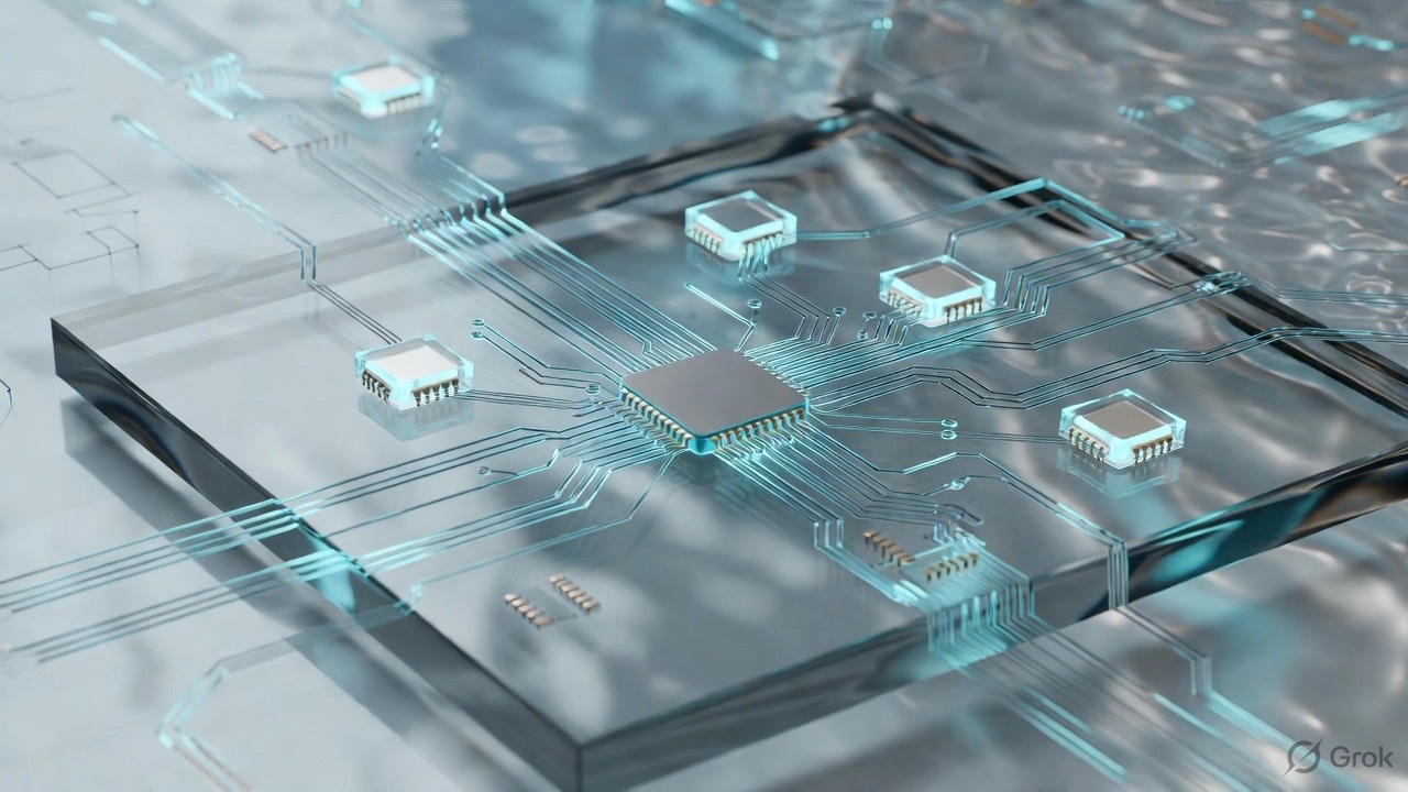
Glass substrates are the next big change in how chips are packaged: replacing the organic base layer that chips sit on with glass, which is flatter and more stable under heat. That stability is what huge AI chips made of many smaller "chiplets" need. Intel is leading, with TSMC, Samsung, Rapidus and SK Absolics expected to follow with mass production around 2027–2028. Intel and its partner 3DGS also plan a roughly US$3.3 billion substrate plant in Odisha, India.
Why the base layer suddenly matters
A modern AI accelerator isn't one chip. It's several chiplets plus high-bandwidth memory, wired together on a substrate. As these packages get bigger and run hotter:
- Organic substrates warp, which limits how big and dense packages can get.
- Glass stays flat and dimensionally stable, allowing finer wiring and larger packages.
- Better signal and power delivery become possible across the package.
Analysts describe organic materials as approaching their physical limits for this kind of high-end chip.
Where things stand
- January 2026: Intel showed the first sample combining its EMIB packaging with a glass substrate at NEPCON Japan, and reported no micro-cracks in testing.
- 2026–2030: Intel's stated window for broad use.
- India: the planned Intel–3DGS plant in Odisha is expected to take five to six years to build.
Some coverage makes dramatic performance claims that haven't been independently verified, so treat headline multipliers with caution.
Why I'm writing about chip packaging
Because it's part of why AI keeps getting cheaper. Better packaging means more capable accelerators per data-centre rack, which feeds through to lower costs for the AI APIs that small businesses build on. India hosting part of that supply chain is good news for the wider tech ecosystem here too.
At NextGen Fusion, our software and AI development company in Lucknow, we build products that benefit from that curve: AI features that get faster and cheaper as the hardware improves.