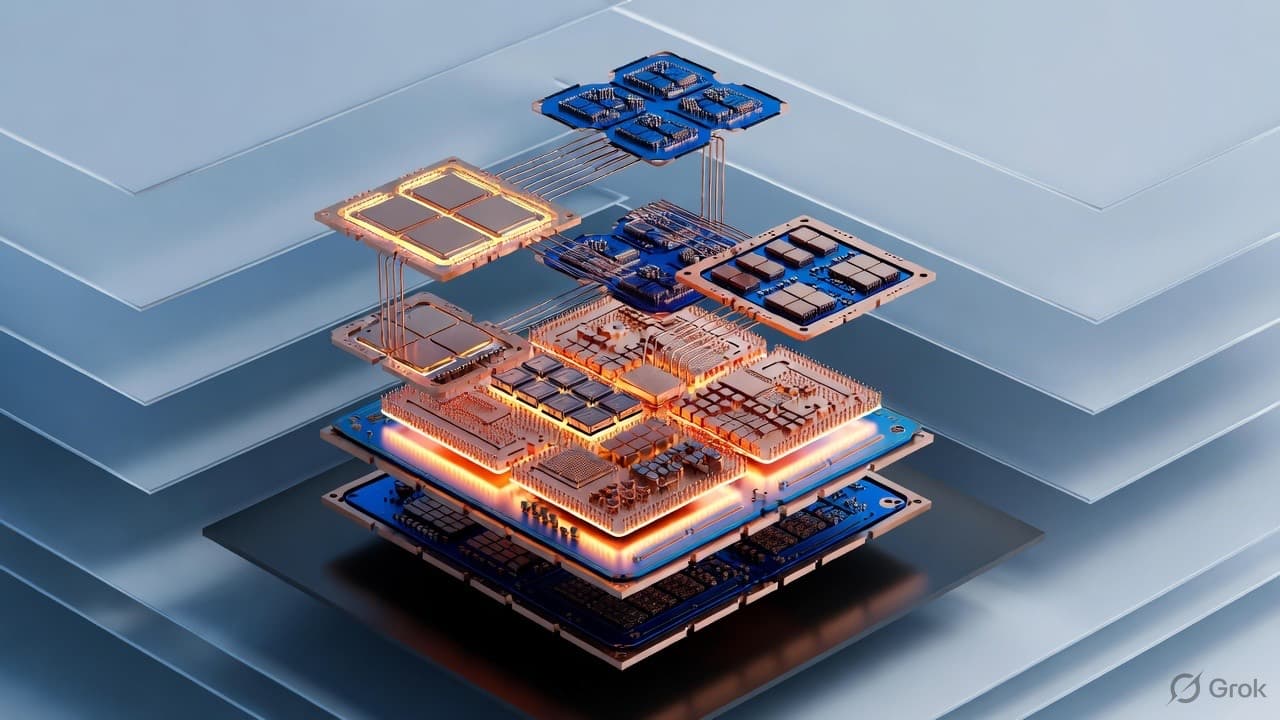
Modern AI chips aren't single pieces of silicon. They're several "chiplets" plus stacks of high-bandwidth memory, joined together by advanced packaging technologies like TSMC's CoWoS and Intel's EMIB. In 2026, packaging capacity rather than chip fabrication has become one of the tightest bottlenecks in AI hardware, with TSMC's CoWoS widely reported as sold out and the company reportedly outsourcing some packaging work to partners like ASE and Amkor.
Why chiplets and advanced packaging
Making one giant chip is expensive and wasteful: a single defect ruins it. Splitting a design into smaller chiplets and connecting them closely gives:
- Better yields and lower cost per working chip.
- Mix and match: compute, I/O and memory can use different processes.
- Huge bandwidth between processor and memory, which is exactly what AI needs.
The main technologies
- TSMC CoWoS (Chip-on-Wafer-on-Substrate) places chips and HBM side by side on a silicon interposer. It's the workhorse behind most leading AI accelerators.
- Intel EMIB uses small silicon bridges embedded in the substrate instead of a full interposer. Some chip designers are reportedly testing it as an alternative while CoWoS is constrained.
- Next up: panel-level packaging and glass substrates, both aimed at bigger, denser packages later this decade.
How tight is capacity?
Reports differ on the numbers. Estimates for TSMC's CoWoS capacity range from roughly 115,000 to 140,000 wafers a month by the end of 2026, with plans reported to roughly double by 2028. None of it is confirmed by TSMC, so treat the figures as directional. The consistent message is that demand still outruns supply.
Why software builders should care
Packaging limits how many AI accelerators reach the market, which affects how quickly AI inference gets cheaper. India's growing packaging industry (the Sanand cluster) is part of the global response.
At NextGen Fusion, our AI and software development company in Lucknow, we build AI features to benefit as that capacity arrives: model-agnostic, cost-aware and easy to upgrade.